Application Introduction
Supports full manufacturing flow for SiC and GaN wide-bandgap semiconductors: crystal growth, epitaxy, high-energy ion doping, high-temperature activation annealing and device high-voltage testing for EV power devices, PV systems and 5G RF components.
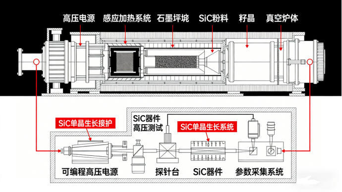
Core Power Function
1. High-current high-voltage power for SiC crystal growth with precise temperature control above 2000°C;
2. Over 200kV ultra-stable acceleration voltage for deep implantation doping;
3. High-temperature annealing power for dopant activation;
4. Programmable high voltage for device breakdown and avalanche testing.
Advantages
Continuous high-power output, temperature accuracy ±0.5%, long-term reliability, fully customizable for domestic third-gen semiconductor equipment.
Working Principle
High-stability power ensures ultra-high temperature crystal growth and provides full-process high voltage for ion implantation, annealing and electrical testing to guarantee device performance and yield.
Application Fields
SiC crystal growth, GaN epitaxy, automotive-grade SiC power devices, 5G RF GaN components.