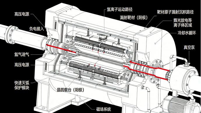
Application Introduction
Magnetron sputtering is the core wafer metallization process. High-energy ions eject target atoms to form uniform metal interconnects, barrier layers, seed layers and bump layers on wafers. It supports aluminum, copper, titanium, gold and nichrome targets for wafer fabrication and advanced packaging.
Core Power Function
1. Apply negative high voltage to targets to ignite argon glow discharge plasma;
2. Accelerate argon ions for stable target sputtering;
3. Excellent arc suppression reduces particle defects and ensures uniform thin-film deposition.
Advantages
Ripple below 0.1% peak-to-peak, 1μs fast arc extinguishing, low arc current, suitable for single or multi-target co-sputtering and reactive sputtering.
Working Principle
Negative high voltage generates argon plasma in vacuum. Accelerated ions bombard targets to deposit dense nano metal or dielectric films uniformly on wafer surfaces.
Application Fields
Metal interconnect deposition, photomask coating, advanced packaging bump fabrication, ohmic contact layers for compound semiconductors.