Application Introduction
Plasma etching is the core pattern transfer process for advanced manufacturing below 28nm. It includes CCP capacitive coupled etching for high aspect ratio dielectric etching and ICP inductive coupled etching for low-damage silicon and metal etching. Nano-scale patterns are precisely transferred on wafers through physical ion bombardment and chemical reactions, which is essential for logic chips and 3D NAND memory production.
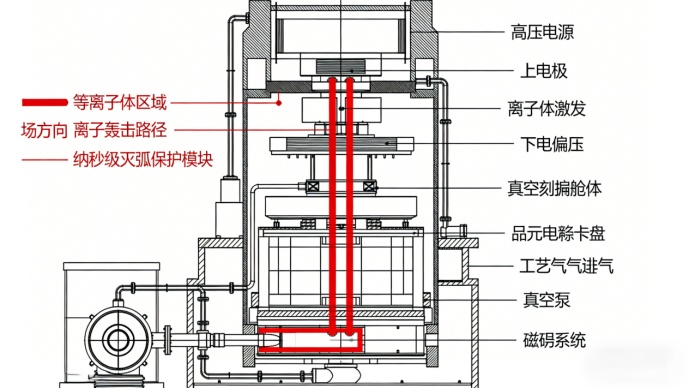
Core Power Function
1. Supply RF high voltage to upper electrode to generate high-density fluorine or chlorine plasma inside the chamber;
2. Provide bias high voltage for wafer stage to form directional electric field and ensure anisotropic etching with vertical ion bombardment;
3. Nanosecond arc suppression prevents wafer damage caused by plasma arcing.
Advantages
Nanosecond arc recovery, wide frequency and power linear adjustment, fast impedance matching, fully compatible with domestic etching equipment localization.
Working Principle
High-voltage power generates dense plasma while wafer bias forms directional ion flow. Energetic ions bombard vertically with chemical radicals to achieve high-precision anisotropic nano etching.
Application Fields
Advanced logic etching, 3D NAND deep trench etching, power device trench etching, MEMS structural etching.