Application Introduction
Scanning Electron Microscopes (SEM) deliver high-resolution micro-morphology characterization for wafer defect inspection and chip failure analysis. Focused electron beams scan samples to collect secondary and backscattered electron signals for nanometer-level imaging widely used in semiconductors, materials science, geology and biomedicine.
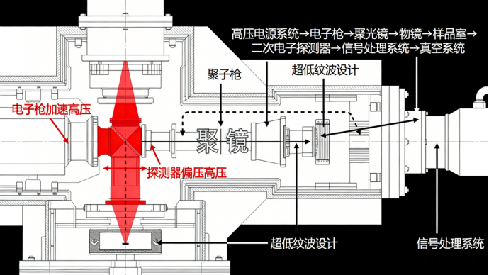
Core Power Function
1. Provide ultra-stable 1kV~30kV accelerating high voltage for electron guns to form collimated electron beams;
2. Support matched high voltage for electromagnetic lenses and scanning deflection systems for precise focusing;
3. Supply detector bias voltage to enhance signal collection efficiency.
Differentiated Advantages
ppm-level long-term stability, ripple ≤10mVpp, ultra-low noise and strong anti-interference, compact integration suitable for domestic tabletop and floor-standing SEM equipment.
Working Principle
Ultra-stable accelerating voltage focuses electron beams onto samples to generate secondary and backscattered electrons. Detector bias amplifies weak signals to reconstruct nanoscale high-resolution surface morphology images.
Application Scenarios
Wafer defect inspection, chip failure analysis, microstructure characterization, nanomaterial research and geological mineral testing.