Application Introduction
X-ray analytical instruments are essential for semiconductor material characterization and industrial non-destructive inspection. They include XRD for crystal orientation and structure analysis, XRF for quantitative elemental composition, industrial CT/DR for packaging void and solder joint inspection, and X-ray thickness meters for nanometer-level thin-film measurement across semiconductors, lithium batteries and metallurgy industries.
Core Power Function
1. Deliver highly stable 0~60kV DC high voltage for X-ray tubes to accelerate electrons and generate characteristic X-rays;
2. Adjustable filament power precisely controls tube current for linear X-ray dosage regulation;
3. Bias high voltage improves detection sensitivity for receiving sensors.
Differentiated Advantages
Tube voltage/current precision ≤0.1%, stability ≤±0.005%, full overvoltage/overcurrent/filament protection, compact size compatible with desktop and inline inspection machines.
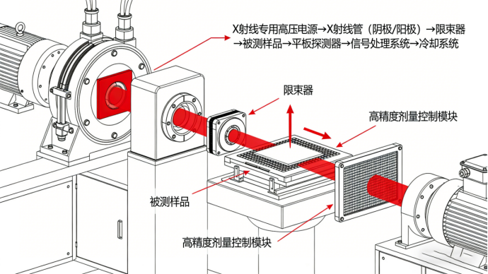
Working Principle
Controlled high voltage accelerates electrons toward the anode target to produce characteristic X-rays. After penetrating samples, signals are collected and processed to analyze crystal structures, chemical composition and internal defects non-destructively.
Application Scenarios
Wafer crystal orientation analysis, packaging solder defect detection, thin-film thickness measurement, material composition analysis and industrial non-destructive testing.