Atomic Force Microscope (AFM) is a tool used to study the surface morphology and nanostructure of various solid samples at the nanometer to micrometer scale. Common core samples include:
① Inorganic hard materials: silicon wafers, wafers, metals, ceramics, graphene, etc.
② Organic polymer materials: polymer films, polymer fibers, polymer composite materials, etc.
③ Biological related materials: proteins, DNA, bacteria, biofilms, medical implant materials, etc.
④ Others: micro-nano materials, electrode materials, etc.
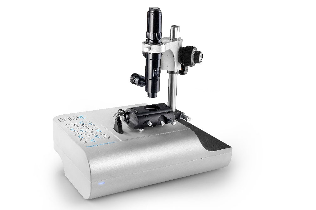
Product Information
The basic principle of AFM utilizes a micrometer-scale cantilever spring with a conical probe at its free end. The probe tip is extremely sharp, with a curvature radius typically less than 10 nanometers, scanning the sample surface at an extremely close nanometer distance.
As the probe moves across the sample surface, the van der Waals force between atoms at the probe tip and atoms on the sample surface changes, causing vertical displacement of the cantilever.
The laser beam reflected from the back of the cantilever irradiates a quadrant photodiode. The output signal of the photodiode corresponds to the vertical movement of the cantilever, thereby reflecting the surface topography of the sample.
Meanwhile, the main functions of AFM include high-resolution imaging, mechanical property characterization, and electrical performance characterization. Therefore, AFM is widely applied in three major fields:
① Semiconductor & Electronics Industry: Cross-sectional analysis of samples such as wafer sections, silicon wafer sections, and semiconductor device sections; defect detection, device leakage analysis, and characterization of wafer structures or electrode surface topography.
② Biomedical & Life Sciences: Cell research including macromolecular structure analysis and micro-nano topography observation of living cell surfaces; characterization of biomaterials for biomarker detection and pharmaceutical research & development.
③ Materials Science & New Energy: Analysis of micro-nano morphology for inorganic, organic and composite materials; structural optimization and performance improvement for photovoltaic, catalytic, lithium battery and energy storage materials.
The independently developed AFM by Dalian Feimate Nanotechnology Co., Ltd. is specially designed for high-end quality control. It is highly suitable for solar cells, semiconductors & integrated circuits, surface engineering & materials science, ceramics & coatings, polymers & chemical products, nanoscale mechanical & electrical performance testing, pathology & drug synthesis research, and biotechnology applications.
II. Advantages of AFM
① Compact size with elegant modern design
Feimate’s self-developed AFM features an ingenious compact structure that occupies minimal laboratory space. Its aesthetic appearance is widely recognized and favored by users.
② Simple operation with excellent user-friendliness
Feimate AFM is extremely easy to operate and compatible with all types of computers, including desktops, all-in-one PCs and laptops. With LAN connectivity, all data transmission between the device and a computer can be completed using a single network cable.
③ High efficiency with fast nano imaging
Simplified nano imaging workflow greatly shortens the overall scanning time.
Optimized leveling process enables precise probe alignment in the shortest possible time.
The built-in high-performance optical microscope allows initial positioning and selection of scanning points.
Adopting the latest advanced electronic technology significantly improves the operating performance of the new-generation controller.
Fast approaching technology greatly accelerates the testing process, serving as one of the core highlights of Feimate AFM.
④ Easy installation with sturdy durable structure
III. Assembly & Operation Guide
Take the microscope stage out of the package and place it on a flat desktop.
Remove the test platform, adjust the side knob to expose the front and rear screw holes, place the platform on the microscope stage, and fasten it with four short screws using the provided wrench.
Take out the microscope base, align it with the screw holes on the test platform, and secure it with four long screws.
Attach the ring clamp to the microscope base and tighten the front knob to fix it.
Insert the camera bracket into the microscope base and fasten the front knob.
Take out the vertical microscope unit; disconnect the adapter and power cable first, place the probe unit into the bracket, reconnect the power cable, and lock the front knob.
Take the positioning head from the accessory box and place it on the three support points of the AFM. Fix the rear two points first, adjust the front support to keep the head stable, then connect all cables.
Connect the foot pedal cable to the vacuum device; place the vacuum tool and probes on the desktop and position the foot pedal on the floor.
Connect the AFM controller to the power supply on one side and to the vertical probe cable on the other side.
Connect the camera cable from the camera top to the computer.
Plug the device adapter into the power socket and connect it to the AFM main unit.
Connect the yellow Ethernet cable from the computer USB network adapter to the AFM device.
IV. Sample Adjustment & Preparation
Remove the positioning head from the box, flip it front-to-back, and place the cable side aligned with the notch inside the box.
Slide the side switch of the positioning head to open the probe locking lever of the AFM scanner.
Take the sample sheet from the transparent sample box, gently pick it up using the vacuum probe, place it in the center of the sample holder, and ensure full contact without tilting or suspension.
Close the probe locking lever by toggling the side switch again.
Place the positioning thin plate onto the scanner base, then install the entire positioning head steadily.
AFM Specifications
Scanner
XY Scanner:
Max scanning range: 50μm
Resolution: 1nm
Z Scanner:
Max scanning range: 4μm
Resolution: 0.1 nm
Electronic System
4-channel 24-bit ADC
4-channel 24-bit DAC
Signal Processing
40MHz high-frequency processor
Integrated Functions
10/100/1000 Mbps LAN interface
Stage
XY Stage:
Motorized software-controlled positioning stage
Travel range: 15 mm
Step resolution: 40 nm
Z Stage:
Travel range: 15 mm
Step resolution: 40 nm
Automatic fast approaching for micro-cantilever
Software
Data Acquisition
Real‑time 100 Mbps, compatible with Windows 10
Integrated optical view for probe & sample visualization
Image Processing
Independent software for analysis, rendering & reporting
Supports export of multiple image formats
Fully compatible with all Windows operating systems
Sample Mounting
Max sample diameter: 20 mm
Max sample thickness: 10 mm
Magnetic sample holder included
Sample bias voltage range: -10V ~ +10V
Recommended PC Configuration
21.5‑inch all‑in‑one monitor
Intel Core i5‑7500 CPU
8GB DDR4 RAM
1920×1080 Full HD resolution
Top View Microscope
8MP color camera
Optical zoom: 60× ~ 600×
Integrated LED lighting
Field of view: 260μm² ~ 2.6mm²
AFM Main Unit
Dimensions
300 mm × 400 mm × 300 mm
Weight
20 kg (excluding packaging)
Probe Module
Precise adjustment via micrometer screw
Laser wavelength: 670 nm
Max laser diode power: 5 mW
Options & Accessories
Plug‑and‑play installation
Microscope brightness dimmer
Standard test samples, mounting kits & substrates
Probe replacement kit including vacuum pen, tweezers & storage box